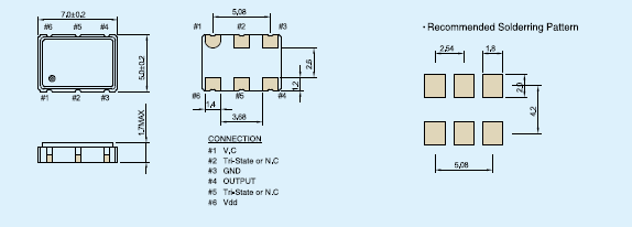


 KVS7 (SMD VCXO 7.0X5.0mm)
 |
• Wide Frequency & Voltage range • Available 3-State function • Available wide pull-range • Excellent heat resistance, high precision, and high stability. • Nominal frequency range : 1MHz to 200MHz • Mode : Fundamental, Multi |
| Standard Specification | |||||
|---|---|---|---|---|---|
| Frequency Range | 1.000MHZ to 200.000MHZ | 1MHZ~60.000MHZ | |||
| Supply voltage | 2.5V | 3.3V | 5.0V | ||
| Pin 1 Control voltage | 1.25V±1.05V (1.25V) | 1.65V±1.35V (1.65V) | 2.5V±2.0V (2.5V) | ||
| Frequency Deviation | ±50ppm min, ±100ppm min, ±150ppm min (option) | ||||
| Linearity | 10% max | ||||
| Slope | Positive | ||||
| Current consumption | 40㎃ max | 50㎃ max | 35㎃ max | ||
| Temperature Range | Operating | -40℃ to +85℃, User spec | |||
| Storage | -55℃ to +125℃ | ||||
| Frequency Stability | ±50ppm max, User spec | ||||
| Output load condition(CMOS) | CMOS 15pF | ||||
| Symmetry (Duty) | 45% to 55% (1MHZ ~70MHZ max) 40% to 60% (70.001MHZ ~200MHZ max) | ||||
| Output rise and fall time (tr/tf) | 5ns max | ||||
| High output voltage (CMOS) | 90% Vdd | ||||
| Low output voltage (CMOS) | 10% Vdd | ||||
| Pin 2 Input voltage | No Connection (Enable Output) | ||||
| Pin 5 Input voltage | 70% Vdd min (Output enable) | ||||
| Pin 5 Input voltage | 30% Vdd max (Output disable) | ||||
| Oscillation start up time | 5㎳ max | ||||
| Aging | ± 3ppm max | ||||
| phase Jitter (12KHZ ~20MHZ) | 100ps max | ||||
| Period Jitter (Pk-Pk) | 25ps max | ||||